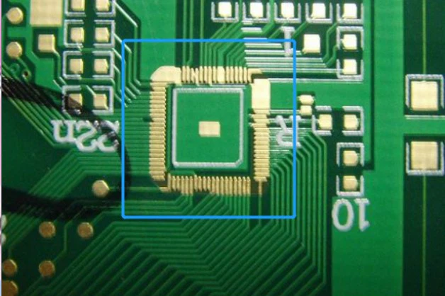
According to the way of surface treatment, it can be divided into the following 2 types: Immersion Gold, Ni/Pd/Au. Immersion Gold The deposition thickness of nickel is 120 ~ 240 μinch (about 3 ~ 6μm), and that of gold is 2 ~ 4μinch (0.05 ~ 0.1μm) Advantages: 1. The Immersion Gold PCB surface is very flat and coplanar, which is suitable for the contact surface of keys. 2.The solderability of the gold deposit is excellent, and the gold will quickly melt into the molten solder to form metal compounds. Disadvantages: high cost, and strict control of process parameters (smooth metal surface, strict bonding parameters, etc.) is required to achieve a good bonding effect. The gilded PCB surface is easy to produce black plate benefit (nickel corrosion), which affects the reliability of final welding and the problem of desoldering. Ni/Pd/Au Nickel thickness is 120~240μInch (about 3-6 um), the thickness of palladium is 4~20μ Inch (about 0.1~0.5 um); The thickness of gold is 1-4 μinch(0.02~0.1 um) Advantages: Compared with immersion gold, nickel palladium gold can effectively prevent connection reliability problems caused by black disk defects, and is widely used in middle and high-end products. Disadvantages: Although nickel palladium gold has many advantages, palladium is expensive and costly. Process control requirements are strict. !page-628-418 Processing capacity of bonding boardsProcessimmersion goldNi/Pd/Au Line width/spacing(um) 75/75um 75/75um Bonding Pad size(um) 75200um 100200um Flatness of bonding position Gold surface flatness requirements are strict Gold surface flatness requirements are strict(A slight scratch is acceptable) !page-216-210 AVI Machine