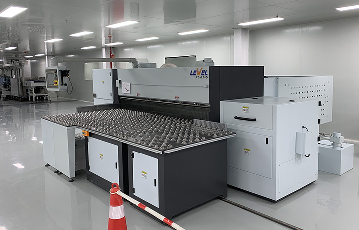
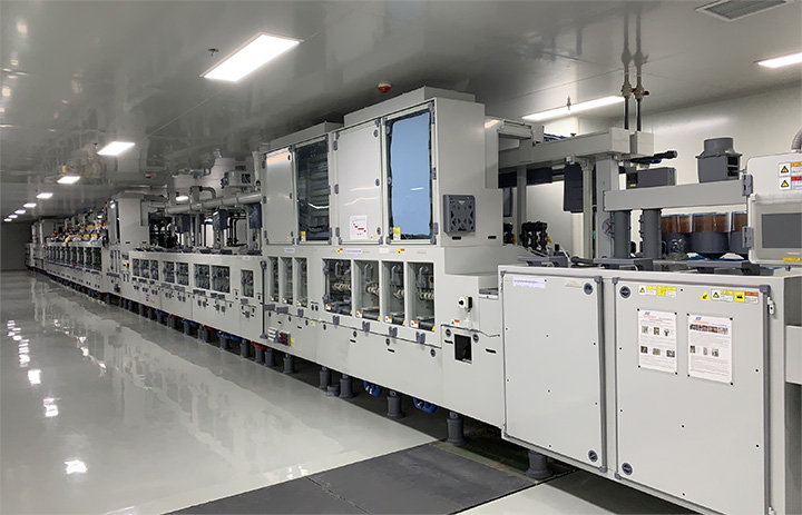
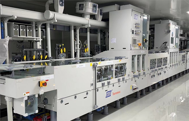
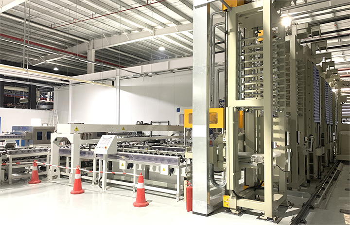
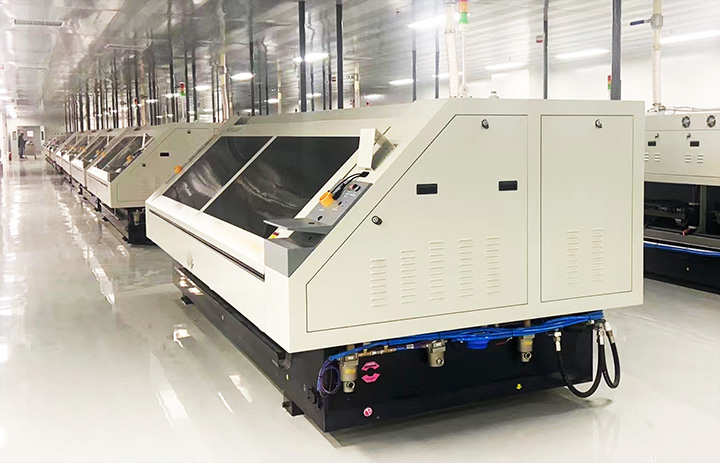
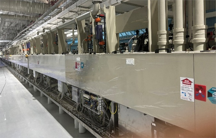
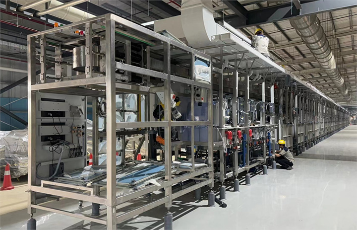
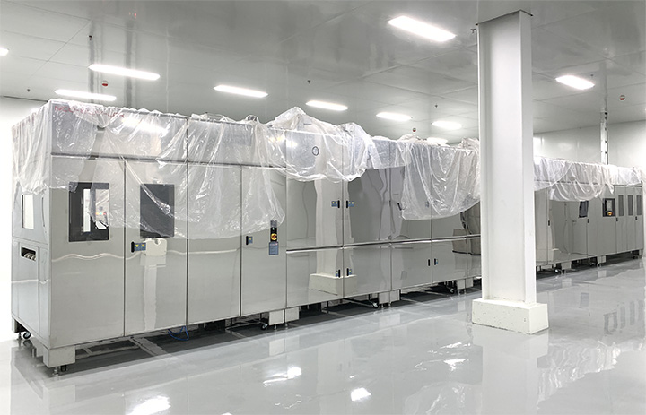
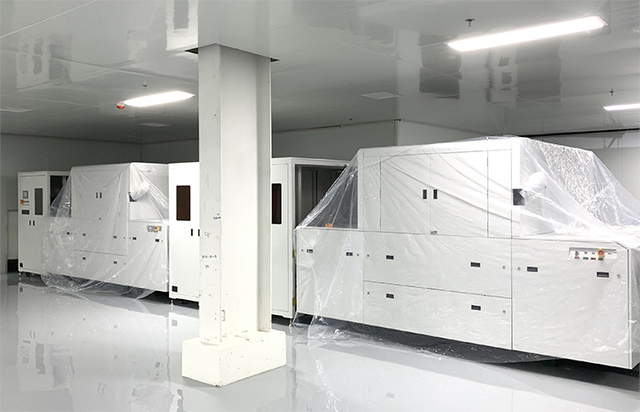
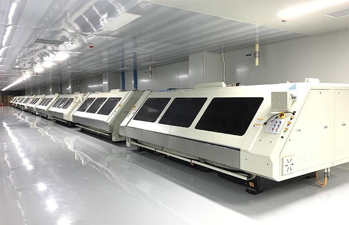
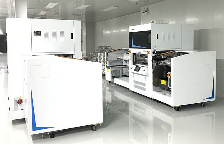
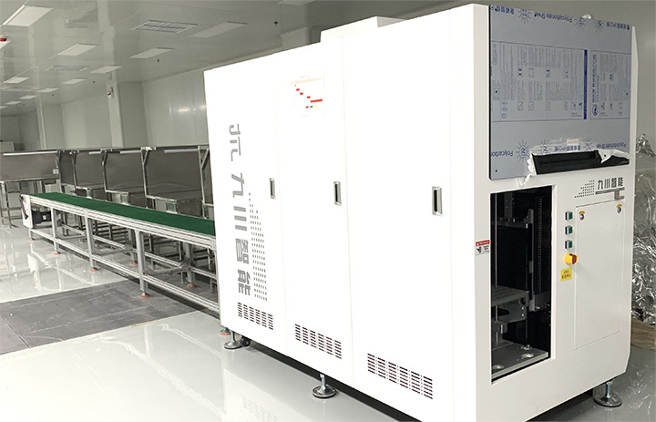
Core Competency / Capabilities

Engineering
Excellence

15+ years of precision PCB fabrication. From prototype to high-volume production, FQC delivers multilayer, HDI, heavy-copper, and high-speed low-loss PCBs under nine ISO/IECQ/IATF certifications.

Manufacturing Specs

REF-SPEC-2026
Multilayer Rigid
Max Layers100+
Board Thickness0.4 – 6.5 mm
Aspect Ratio20:1

Parent spec · production-validated

Advanced HDI
Build-Up Order5th-Order Any-Layer
Min Laser Via3 mil (0.075 mm)
HDI Max Layers16L Any-Layer
Heavy Copper
UL-Listed (2L)15 oz
UL-Listed (Multilayer)13 oz
Primary ApplicationsEV · Solar Inverters
High-Speed / Low-Loss
MaterialsMegtron 6/7/8 · Rogers
Impedance Tolerance±5% (industry ±10%)
Max Frequency40 GHz
Detailed Specification

Full spec sheet.

ParameterValueNotes
Max layers100Parent spec · production-validated
Board thickness0.4 – 6.5 mmRigid
Min trace / space2 mil / 50 μmProduction-grade
Min mechanical drill6 mil (0.15 mm)
Min laser via3 mil (0.075 mm)CO₂ or UV
Max aspect ratio20:1Mechanical through-hole
Impedance tolerance±5%vs. industry ±10%
Max copper weight15 oz outer / 13 oz innerUL-listed
Max frequency40 GHzMegtron / Rogers / Taconic
Surface finishesENIG, ENEPIG, OSP, HASL, Immersion Silver, Gold Fingers
HDI build-up orderUp to 5th-order Any-Layer
HDI max layers16Any-Layer

Source: parent-company (Sihui Fushi) published capabilities, fsqualitypcb.com

The Fabrication Lifecycle

Every board moves west-to-east through a single 12-station flow. Each station is gated against ISO/IATF process parameters before advancing.

12 Stations9 Certifications
01

CCL Cutting

Copper-clad laminate sheet cutting from raw stock.

CCL Cutting MachineRaw material feed
02

Inner-Layer LDI Imaging

Direct laser imaging of inner-layer circuits.

LDI / Auto DeveloperMin 2 mil trace
03

DES Line

Develop, etch, and strip of inner layers.

DES Auto LineClosed-loop etchant control
04

Inner AOI

100% automated optical inspection of each panel.

AOI StationsFull-panel inspection
05

Brown Oxidation

Copper surface treatment before multilayer bonding.

Brown Oxidation BayBond-strength prep
06

Vacuum Lamination

Multilayer stack bonding under heat and pressure.

Vacuum Lamination PressProgrammable thermal profile
07

Drilling (Mechanical + Laser)

Through-hole and microvia drilling.

CNC Drill + CO₂/UV LaserMech 6 mil · laser 3 mil
08

Chemical Plating

Desmear and electroless copper deposition.

Chemical Plating LineThrough-hole continuity
09

Electroplating (VCP)

Vertical continuous plating for copper thickness.

VCP Electroplating LineHandles 20:1 AR
10

Solder Mask + Cure

Photoimageable solder resist apply and cure.

Solder Mask LineLDI-exposed
11

Legend Printing

Reference-designator inkjet printing.

Legend Inkjet PrinterNon-contact
12

Outline → E-Test → AVI/FQC

V-cut/rout, 4-wire flying-probe e-test, AVI + X-ray final, packaging.

V-cut / 4-wire FP / AVI / X-ray100% electrical test

The Equipment Stack

A single 406 × 60 m production building houses the full 12-station line. 24 robotic arms handle inter-process transfer — boards never leave the line.

CCL Cutting Machine
01CCL Cutting Machine
DES Auto Line
02DES Auto Line
Brown Oxidation
03Brown Oxidation
Vacuum Lamination Press
04Vacuum Lamination Press
Mechanical + Laser Drilling
05Mechanical + Laser Drilling
Chemical Plating Line
06Chemical Plating Line
VCP Electroplating Line
07VCP Electroplating Line
Solder Mask Line
08Solder Mask Line
Legend Inkjet Printer
09Legend Inkjet Printer
Outline Rout / V-Cut
10Outline Rout / V-Cut
4-Wire Flying Probe E-Test
114-Wire Flying Probe E-Test
AVI / X-ray Final QC
12AVI / X-ray Final QC
Materials Supported

Qualified base materials.

Stocked inventory of 8+ high-reliability laminates matched to customer Dk/Df and impedance specs. Hybrid PTFE stack-ups built to print on request.

FR-4 High-TgPanasonic Megtron 6Panasonic Megtron 7Panasonic Megtron 8Rogers RO4350BRogers RO3003Taconic RF-35Isola FR408HRPolyimide FlexHybrid Stack-UpsBT ResinPTFE

Coming soon — contact sales for detailed spec requirements.