Where FQC Specializes
FQC runs the same flow as any multilayer fab. What's different is the spec ceiling.
Below are the capabilities where FQC's process library outruns commodity fabs.
Where FQC is not a commodity.
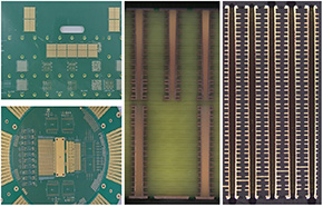
Multilayer product — FQC
ULTRA-HIGH LAYER COUNT
Up to 100 Layers
Traditional PCB fabrication tops out at 32–48 layers. FQC's parent has shipped 100-layer boards for AI-server backplanes and test fixtures.
Three things have to hold simultaneously: a 20:1 mechanical-drill aspect ratio, ±5% impedance control across all 100 layers, and press-cycle dimensional stability. Lose any one and the yield collapses — that is why fewer than five non-China bases carry this capability.
Goes into AI-training backplanes, SerDes midplanes, and ATE IC test boards. Disclosed sector: AI / server end customers.
Max layer count
100
Aspect ratio
20:1
Impedance tolerance
±5%
Layer-to-layer registration
±25 μm (multilayer)
42-layer ATE test board · 2024 Guangdong Outstanding Hi-Tech Product award
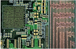
HDI product stack — FQC
HIGH-DENSITY INTERCONNECT
5th-Order Any-Layer HDI
Any-layer HDI up to 16 layers, five sequential lamination cycles, microvias stacked or staggered. Most fabs stop at 2nd-order, 8–10-layer any-layer.
This is smartphone-density routing at PCB scale. Positional error multiplies with every lamination cycle, so dimensional control and laser-via-to-land alignment have to hold through the entire flow, not just the first pass.
Goes into 800G / 1.6T optical modules, AI accelerator carriers, and high-density BGA escape. Disclosed sector: leading optical-module end customer (anonymized).
Build-up order
Up to 5th-order any-layer
Max HDI layers
16L any-layer
Min laser via
3 mil (0.075 mm)
Representative stack
3+4+3 HDI
800G qualified Oct 2024 · 1.6T qualified 2026 · 3+4+3 HDI with embedded Cu blocks
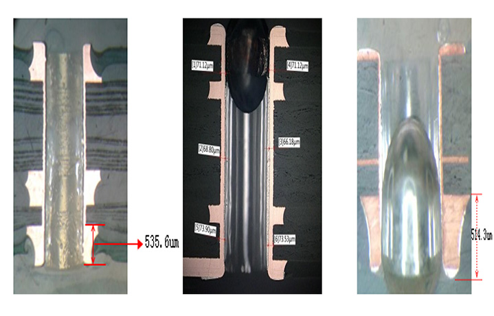
Heavy copper product — FQC
HEAVY COPPER
15 oz Heavy Copper (UL-listed)
Outer-layer 15 oz and inner-layer 13 oz, both UL-listed. Most fabs stop at 6 oz; PCBWay at 13 oz.
Required anywhere DC current has to move at scale — EV battery management, solar/wind inverters, industrial power supplies, EV charging. Thick copper simultaneously stresses etch definition, via reliability, and plating uniformity.
Goes into EV BMS, solar inverters, industrial motor drives, and EV charging stations.
Outer copper
15 oz
Inner copper
13 oz
UL listing
2L and multilayer
Industry benchmark
+15% vs PCBWay 13 oz
PCBWay ceiling 13 oz · FQC 15 oz — 15 % above the reference spec
High-speed signal test — FQC
SIGNAL INTEGRITY
±5% Impedance Tolerance
Twice as tight as the ±10% industry norm. This is the number that decides whether DDR5, PCIe Gen5, SerDes, and 5G mmWave designs work.
Impedance variance collapses the eye opening at high data rates. Trace width, dielectric thickness, copper roughness, and post-lamination glass-weave variation all have to fall inside the ±5% window — and on every board that ships, not a golden sample.
Goes into server motherboards, 5G base stations, and automotive 77 GHz radar. Volume spec, not one-off — every shipped board holds this tolerance, verified via coupon TDR.
Tolerance
±5%
Industry norm
±10%
Applicable geometry
Microstrip / stripline
Target rate
DDR5 · PCIe Gen5 · SerDes
Production-line standard · TDR-verified per lot
High-speed low-loss PCB — FQC
HIGH-FREQUENCY
High-Frequency to 40 GHz
Qualified process flow for Megtron 6/7/8, Rogers RO4350B and RO3003, and Taconic RF-35 — validated in production at up to 40 GHz.
mmWave boards only work when three things come together: ultra-low-loss dielectric, fine-line fabrication, and tight impedance. FQC runs all three on the same line, which is rarer than any single one of them on its own.
Goes into 77 GHz automotive radar, 5G mmWave base stations, and satellite communications.
Qualified materials
Megtron 6/7/8 · Rogers · Taconic
Max frequency
40 GHz
Dielectric loss
Df down to 0.002 (Megtron 8)
Target application
77 GHz radar · 5G mmWave
Full high-speed material stack in production qualification
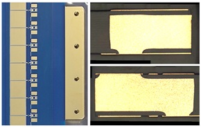
Copper-inlay product — FQC
HYBRID CONSTRUCTION
Heavy Copper + HDI Hybrid
Embedded copper blocks inside an HDI stack. Uncommon enough that most fabs will quote it out.
Needed when a single board has to move power and high-speed signals simultaneously — high-power AI accelerator cards with on-board VRM, or laser driver boards for optical modules. Position tolerance between the embedded block and its surrounding vias has to survive every lamination cycle.
Goes into AI accelerator cards with on-board VRM and laser-driver PCBs for optical modules.
Construction
3+4+3 HDI + Cu block
Embedded Cu block
Embedded pre-lamination
Min line width
2 mil / 50 μm
HDI layer count
Up to 16L
800G optical module · 3+4+3 HDI with embedded Cu blocks · qualified Oct 2024
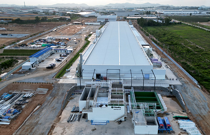
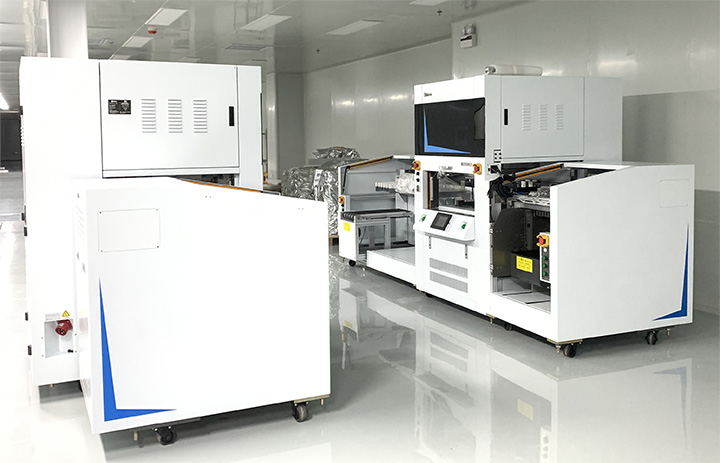
FQC Rayong facility
INFORMATION SECURITY
Information Security (ISO/IEC 27001)
Rare among PCB fabs. Protects customer design IP from the moment Gerbers land to the moment the last panel ships.
Defense, AI, and cutting-edge design customers will not send Gerbers to a fab without 27001. Access control, physical security, log auditing, and staff screening are run with the same rigor as process traceability.
Goes into chip-company reference designs, defense and government work, and any design where IP protection has a real dollar value.
Scope
Design-data handling end-to-end
Standard
ISO/IEC 27001:2022
Obtained
2023
Control set
Annex A · 93 controls
ISO/IEC 27001:2022 · currently active
NEXT STEP
Not sure if your project fits.
Talk to an engineer, or send Gerbers for a DFM review.