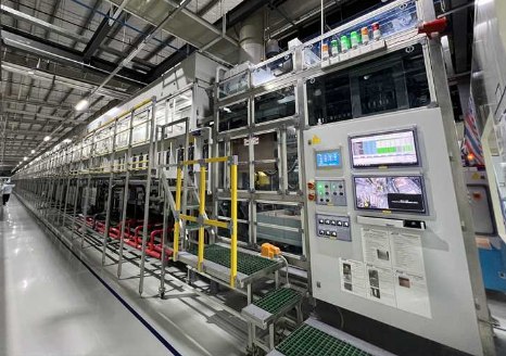
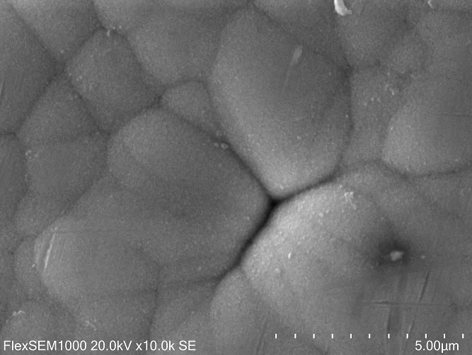
In the manufacturing process of PCB, there are two methods: horizontal copper deposition and vertical copper deposition. These two methods have different advantages and disadvantages in practical applications. Difference Horizontal copper deposition: Horizontal copper deposition refers to the process of immersing the entire board in a copper solution during the production of the PCB, causing copper to deposit on the entire PCB. This method can make the copper thickness of the entire PCB uniform and have high smoothness. Vertical copper deposition: Vertical copper deposition refers to the process of using electrochemical deposition technology to cover only the required part of the PCB with copper, rather than the entire PCB. This method can only deposit copper at the desired location, thus reducing production costs. Horizontal copper depositionAdvantage: 1. Improving the conductivity of PCB: The copper of PCB is definitely not pure copper, and its composition will accept many other elements, which will reduce the conductivity of copper. However, horizontal copper deposition can make the copper layer of PCB at least 99.99% pure, improving the conductivity of PCB. 2. Improve the corrosion resistance of PCB: Due to the thick copper layer of horizontal copper deposition, which can reach over 70um, the PCB can be well protected from oxidation and corrosion. 3. High smoothness of copper layer: Horizontal copper deposition can make the copper layer of the PCB smooth, which has great benefits for the manufacturing and installation of the board. Disadvantages: 1. High cost: Horizontal copper deposition requires covering the entire PCB, so more copper melting solution is required, which naturally leads to a higher cost. 2. High energy consumption: Due to the need to cover the entire PCB with a copper layer, horizontal copper deposition requires more electrical energy, increasing production energy consumption. Vertical copper depositionadvantage: 1. Low production cost: Vertical copper deposition only requires covering the copper at the required location, without the need to cover the entire PCB with copper. Therefore, less copper melting solution is required, resulting in lower production costs. 2. Easy maintenance: Due to the fact that vertical copper deposition only requires copper covering at the required positions, only these areas covered with copper need to be maintained during maintenance, reducing the difficulty of maintenance. 3. Fast production speed: Vertical copper deposition only requires the required part to be covered with copper, so the speed is fast and can improve production efficiency. Disadvantages: 1. Nonconduction of heat: As only the required part is covered with copper, the thickness of the PCB can vary greatly, which affects the heat dissipation performance of the PCB. 2. It is easy to produce tin oxide: in the process of vertical copper deposition, because the copper solution is weakly alkaline, it has strong penetration to tin, and it is easy to react with the tin on the surface to produce tin oxide, which affects the quality and service life of the PCB. Overall, both horizontal and vertical copper deposition have their own advantages and disadvantages. In the actual manufacturing process of PCB, reasonable choices should be made based on specific production needs.