Objective
Develop a selective electroless thick-gold process that can serve as a versatile surface finish. Target: ≥ 0.3 μm gold thickness on the selected area, ≥ 0.1 μm elsewhere.
Problems with existing methods
- Immersion (displacement) gold deposits only 0.03–0.05 μm and is suitable only for solderable pads.
- As nickel is progressively covered by gold, the deposition rate slows; gold thickness rarely exceeds 0.3 μm and density is poor.
- Electroplating requires extra lead-out traces, which become impractical when the routing is dense.
Principle
- The nickel layer drives catalytic reduction. Adsorbed hydrogen atoms accept electrons; atomic hydrogen is supplied by the reductant, then loses electrons and re-enters the solution as H⁺.
- The original wiring and metal layers on the same pad act as electron conductors. Gold ions continuously gain electrons at the gold surface and deposit — analogous to electroplating gold.
Method
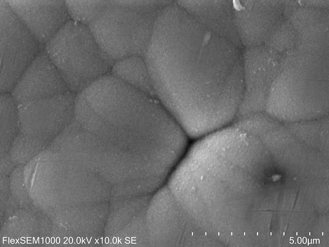
- Step 1 — conventional immersion gold (displacement). SEM at 10,000× shows < 0.02 μm gold. Goal: expose the nickel layer so that reduction electrons can be supplied later.
- Step 2 — apply plating-resist film, leaving only the pads to be thick-gold-plated exposed.
- Step 3 — first electroless reduction gold plating; check SEM at 10,000×.
- Step 4 — strip the plating-resist film.
- Step 5 — second electroless reduction gold plating; check SEM at 10,000×.
Results
| Location | First displacement (thin) | First reduction (thick) | Second reduction (thick) |
|---|---|---|---|
| Selective thick-gold pads | 0.009–0.014 μm | 0.293–0.349 μm | 0.326–0.385 μm |
| Other areas | 0.009–0.014 μm | covered by resist | 0.105–0.111 μm |
Conclusion
The selective electroless thick-gold method meets all target requirements.