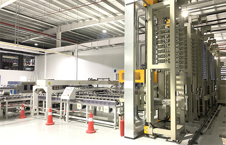
The so-called PCB lamination process refers to the process of overlaying different materials such as boards and laminated materials in layers, heating and drying them under high pressure, and ultimately forming a stable and durable PCB. The entire lamination process consists of multiple steps such as preparing materials, stacking lamination, pressing down, hot compaction, drying, removing residual film, punching, cutting, etc. Firstly, it is necessary to prepare various materials such as plates, laminated materials, residual films, etc. Then stack and compact the boards, laminated materials, etc. According to the parameters such as the structure, number of layers, and thickness of the circuit in the design drawings. This step requires very precise operation to ensure circuit connectivity between different layers. The next step is the pressing process, which involves placing stacked boards, laminated materials, etc. Into a large compactor for high-pressure heating and compaction, so that the materials between each layer are firmly bonded together. After pressing, high-temperature drying is required to remove moisture and volatile substances, making the PCB more stable and durable. Send it into the drying equipment, gradually increase the temperature, and maintain it for a certain period of time. In the process of removing residual film, it is necessary to remove some residues on the surface of the PCB and drill holes to make the circuit connected. The final step is the cutting process, which involves cutting the entire PCB according to the design requirements to meet the product's dimensions and specifications. The lamination process of PCB is an essential step in the manufacturing process of PCB. It can effectively improve production efficiency, ensure product quality and stability. During the manufacturing process, strict adherence to various specifications and operating procedures is required to ensure product quality and the stability of the production process.