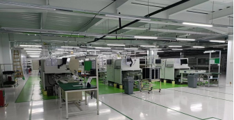
DIP, the abbreviation of dual inline-pin package, is a commonly used packaging technology for electronic components. It is the process of inserting component pins into a plug-in socket and connecting the components to the PCB through welding between the socket and the PCB. DIP packaging has the advantages of simple structure, high reliability, and ease of production and maintenance, making it widely used in the production of various PCB. DIP is commonly used for packaging components such as integrated circuits, diodes, transistors, resistors, capacitors, etc. Specifically, DIP packaging commonly comes in different specifications such as DIP8, DIP14, DIP16, DIP20, and DIP24. Among them, DIP8 is an 8-pin package, usually used in integrated circuits such as operational amplifiers and comparators; DIP14, DIP16, DIP20, DIP24, etc. Are commonly used in digital circuits. The CPU chip packaged with DIP has two rows of pins that need to be inserted into the chip socket with DIP structure. Of course, it can also be directly inserted into PCB with the same number of solder holes and geometric arrangement for welding. Special care should be taken when inserting and unplugging DIP packaged chips from the chip socket to avoid damaging the pins. DIP packaging structures include: multi-layer ceramic dual inline DIP, single-layer ceramic dual inline DIP, lead frame DIP (including glass ceramic sealing, plastic packaging structure, ceramic low melting glass packaging), etc. !DIP layout Characteristic In the era when memory particles were directly inserted into the motherboard, DIP packaging was once very popular. DIP also has a derived method, SDIP, which has a pin density six times higher than DIP. In addition to different packaging specifications, DIP packaging also has three different pin arrangements, namely direct lead, inverted insert, and inverted U-shaped pins. Among them, the direct lead refers to the pin facing 90 degrees downwards or upwards, which is horizontal for the board surface; Inverted insertion means that the pins have a 45 degree or 52 degree angle, which is inclined for the board surface; Inverted U-shaped pins bend the pins into U-shaped shapes on a straight insertion basis. The different pin arrangement makes DIP packaging more flexible and can meet the requirements of different types of components. Purpose The chip using this packaging method has two rows of pins, which can be directly soldered onto the chip socket with a DIP structure or soldered into solder positions with the same number of solder holes. Its characteristic is that it can easily achieve perforation welding of PCB and has good compatibility with the motherboard. However, due to its large DIP packaging area and thickness, and the fact that the pins are easily damaged during insertion and extraction, its reliability is poor. DIP packaging is a very practical packaging technology. Not only is the structure simple, but it also has high reliability, and maintenance and replacement of components are relatively easy. Its widespread application has made the production of boards more efficient and convenient. With the continuous development of technology in the future, DIP packaging technology will also be continuously updated and upgraded to better meet market demands.