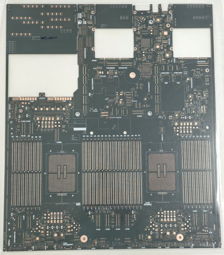
Resin plug-hole technology is increasingly common in PCB manufacturing, especially on high-layer-count, thick-board products. The aim is to fill and plug through-holes during manufacturing to prevent shorts between metal layers.
Principle
In high- and multi-layer PCBs, buried vias are common. Resin plugging means: copper-plate the hole wall, fill the through-hole with epoxy resin, then plate copper again on the surface. The result is a flat board surface with no dimples — the holes are conductive without interfering with soldering.
PCBs have many small holes and protrusions; if they have to be electroplated, those features hurt plating quality, so resin plugging is necessary.
Solder plug vs. resin plug
1. Different processes
- Solder plug — A green coating is added to the elliptical opening of the solder pad to keep solder from wrapping in.
- Resin plug — A hole is drilled in the board and a thermoplastic resin is injected to fill it, protecting the PCB.
2. Different roles
Both aim to prevent electrical-performance degradation:
- Solder plug mainly prevents solder from filling the pad and shorting the internal traces.
- Resin plug mainly provides insulation protection.
After cure, the solder plug shrinks and air pockets form inside the hole — failing to meet the high fill-quality requirements customers want. Resin plugging fills HDI inner-layer buried vias before lamination, eliminating that problem while balancing the conflict between pressed-dielectric thickness control and inner-layer buried-via fill design.
Advantages
Resin plugging is more complex and costlier than solder plugging, but is superior on fullness and quality. It strengthens the PCB mechanically and electrically; by filling irregular holes and gaps, it keeps conductive coatings out of those gaps and prevents adverse reactions. It also leaves the surface smoother, improving mechanical stability and PCB lifetime.
