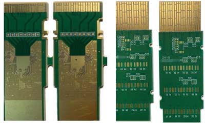
The hole connecting any circuit layer inside the PCB but not conducting to the outer layer is called buried hole.
This process can not be accomplished by pressing and then drilling. It must be performed at the time of individual circuit layers. After pressing the inner layer locally, it must be treated by electroplating before it can be fully pressed, it takes more time than the original"Through hole" and"Blind hole", so the price is also the most expensive. This process is typically used only on high-density circuit boards(HDI) to increase the usable space of other circuit layers.
View the original article on fsqualitypcb.com